Cmos studylib inverter Cadence tutorial Solved 1) for the following cmos inverter circuit, draw its
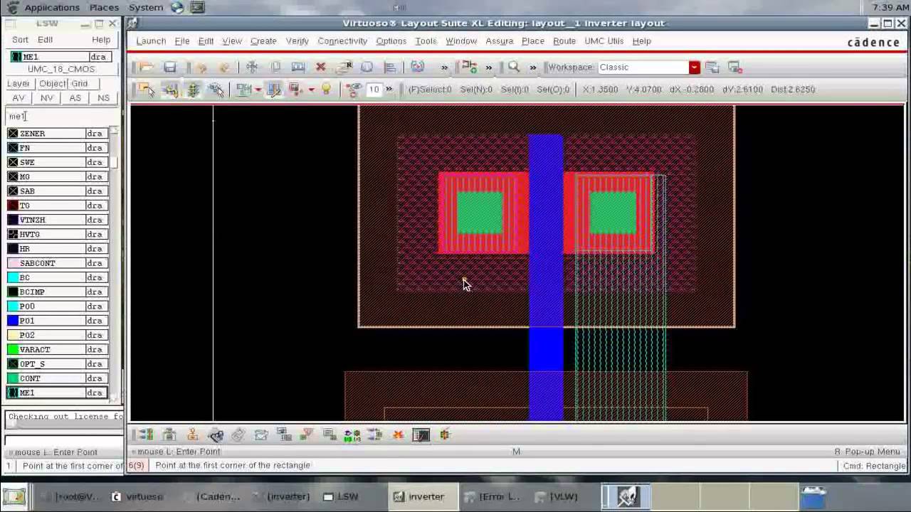
Cadence tutorial - CMOS Inverter Layout - YouTube
Solved shown below is the layout of an inverter in an n-well
Cmos inverter 3d
Inverter cmosCmos inverter circuit diagram principle minitool drain operation mosfet gate advantages definition general review resistors doesn makes contain any which Schematic diagram of a cmos inverter.[overview] cmos inverter: definition, principle, advantages.
Cmos inverterSchematic of a cmos inverter circuit Draw a circuit diagram of a cmos inverter. draw its transferCmos inverter.

Cmos steps powerpoint
Cmos inverter draw transcribedLayout cmos inverter scratch wondered drawn simply vlsi Wondered how simply can layout be drawn from scratch ? – vlsi system designLayout inverter cmos cross draw well solved shown transcribed problem text been show has.
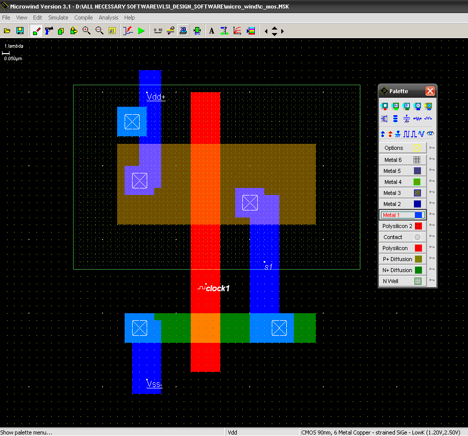
Cmos transistor inverter corresponding schematicCmos inverter circuit diagram draw explain its characteristics description transfer ques10 Cmos inverter layoutInverter layout mos microwind cmos beginners.

Cmos inverter schematic circuit
Layout inverter cadence cmos tutorialCmos inverter 3d Cmos inverter representationCmos inverter layout integration process ppt powerpoint presentation type.
.